rbAmp Wire-Protocol Reference (v1.3)
Audience: 3rd-party and advanced integrators writing their own I²C drivers for the rbAmp module without using client libraries (Arduino / ESP-IDF / Python / ESPHome).
Scope: canonical wire protocol of the rbAmp module at version v1.3 — register map, protocol sequences, behavioral guarantees. This is the complete wire-contract-level reference documentation.
NOT in scope: integration with any specific library / OS / framework — read the library documentation for that.
Document status: DRAFT, 2026-06-16. Source of truth:
registers_v2.yamlv1.3 + canonical wire-contract + bench-validated firmware behavior.
1 · Introduction
rbAmp is a compact hardware module for precision measurements of AC mains parameters over an I²C interface. The module behaves as a standard I²C slave with a fixed register map (page-0, 0x00..0xFF). This document describes the wire protocol at the level of registers, commands, and sequences.
1.1 SKU lineup
| SKU | Current channels (N_I) | U channel | Power calculation |
|---|---|---|---|
| UI1 | 1 | yes | P, PF, Q |
| UI2 | 2 | yes | P, PF, Q per channel |
| UI3 | 3 | yes | roadmap — not shipping on the current MCU package |
| I1 | 1 | no | I only (no P/PF/Q) |
| I2 | 2 | no | I only per channel |
| I3 | 3 | no | I only per channel |
I-variants (I1/I2/I3) have no voltage hardware — U_RMS, U_PEAK, and P registers return 0.0. Frequency (AC_FREQ) is available on all variants (ZC-sourced).
Calibration is factory. The consumer master does NOT configure noise floor (NF), gain, phase compensation, or any other factory parameters — these are all factory calibration burned into the module (see §4.0 reserved ranges). The consumer writes only SENSOR_CLASS + CT_MODEL (see §6.2) — the module applies everything else automatically from the preset table.
1.2 Versioning
| Field | Value |
|---|---|
protocol_version |
1.3 |
schema_version |
2 |
VERSION register (0x03) |
0x04 for v1.3 |
| Page-0 contract | frozen at v1.3 release |
2 · Bus protocol basics
2.0 Power & supply
| Parameter | Value |
|---|---|
VCC nominal |
+5 V |
VCC range |
4.5..5.5 V |
| Typical current draw | ~15 mA |
| Peak current draw (latch + flash write) | ~25 mA |
| Boot inrush | ≤ 50 mA @ 5 ms |
| Sequencing | VCC may be applied concurrently with I²C; pull-ups (3.3 V) are permitted before VCC is applied |
| Isolation | the mains side is galvanically isolated inside the module |
Four wires are mandatory on the LV side:
VCC,GND,SDA,SCL.DRDY(open-drain) is optional. See §2.3 for pull-up and multi-module guidance.
2.1 I²C parameters
- Default address:
0x50(7-bit). - Allowed address range:
0x08..0x77(standard I²C reserved boundaries). - Logic levels: 3.3 V (5 V-tolerant on pull-ups to 3.3 V).
- On-board pull-ups: 4.7 kΩ on SDA/SCL to 3.3 V (module).
- Clock stretching: the module does NOT use SCL clock-stretching as a routine flow-control mechanism. Between transactions the master must observe an inter-transaction gap ≥ 100 µs (
tBUF). Back-to-back transactions without a gap (back-to-back START withouttBUF) are permitted but discouraged — some host stacks (ESP-IDF i2c_master) exhibit an elevated NACK rate. See §5 acceptance / EMI section separately.
2.2 Bus speed
| Speed | Applicability | Note |
|---|---|---|
| 50 kHz | recommended | The ESP-IDF host-side driver shows ~20 % NACK rate at 100 kHz; 50 kHz + 3× retry gives < 0.8 % error rate. |
| 100 kHz | workable with retry | application-level 3× retry is mandatory. |
| 400 kHz | not validated | do not advertise as supported. |
2.3 Multi-module bus
Several rbAmp modules can share one bus:
- Up to ~16 modules (limited by total bus capacitance ≤ 400 pF at 100 kHz).
- Pull-ups: the on-board 4.7 kΩ pull-ups on every module in parallel overload the sink. Cut the on-board pull-ups on every module except one (or use a PCA9515/9615 I²C buffer).
- Length: up to 0.3 m plain → 100 kHz; 0.3–1 m twisted pair (SDA+GND and SCL+GND in separate pairs) → 100 kHz; > 1 m — I²C buffer; > 3 m — differential bus (PCA9615 / LTC4332).
2.4 Bus polling budget
At 50 kHz a single register-read transaction takes ≈ 200–400 µs. The full RT block for one channel (U + I + P + PF, 4 floats = 16 bytes burst) takes ≈ 5–8 ms per channel.
| Configuration | Bus per cycle | Max polling rate |
|---|---|---|
| 1× UI1, RT block | ~5 ms | 100+ Hz (but the module updates at 5 Hz) |
| 5× UI1, RT block | ~25 ms | 5 Hz |
| 16× I3, RT + period | ~400 ms | cannot keep up with the module |
Rule of thumb: at 50 kHz the comfortable limits are 8–10× I3 or 15–16× UI1 at 5 Hz polling.
3 · Variant model
3.1 HW_VARIANT (reg 0x55, u8, read-only)
Authoritative SKU byte:
| Value | SKU | N_I | Voltage HW |
|---|---|---|---|
0x01 |
UI1 | 1 | yes |
0x02 |
UI2 | 2 | yes |
0x03 |
UI3 | 3 | yes (roadmap, not buildable) |
0x04 |
I1 | 1 | no |
0x05 |
I2 | 2 | no |
0x06 |
I3 | 3 | no |
Any other value → the device is not identified as rbAmp.
3.2 CAPABILITY (regs 0x57/0x58, u16 LE, read-only)
12-bit feature-detection map. This is the canonical way to detect supported features — without numeric version comparison.
| bit | Flag | Meaning |
|---|---|---|
| 0 | EXT_ADDRESSING | extended 16-bit addressing (0xFF prefix) |
| 1 | GC_LATCH | General-Call latch is supported |
| 2 | GC_GROUP_FILTER | GROUP_ID filter is active |
| 3 | DIGEST | digest block (0x70..0x85) is exposed |
| 4 | EVENTS | EVENT_FLAGS is supported |
| 5 | UID_ARBITRATION | UID-based address arbitration |
| 6 | SEAL | UID seal verification (anti-clone) — ⚠ declared for forward-compatibility; the CMD_SEAL (0x33) handler and boot-time UID-seal verification are NOT implemented in v1.4.x firmware. The cap bit may be exposed, but the mechanism is inert. A firmware cycle enabling it is planned. |
| 7 | TWO_PHASE_ADDR | two-phase commit address change |
| 8 | ZC_PHASE_OFFSET = voltage-HW | the module has a U channel |
| 9 | SAVE_USER_CONFIG | CMD_SAVE_USER_CONFIG is available |
| 10 | CLEAR_ERROR | CMD_CLEAR_ERROR is available |
| 11 | IAP | in-application programming (F4 tiers only) |
3.2.1 Canonical CAPABILITY values
| Variant group | CAPABILITY value (u16 LE) |
|---|---|
Current-only (I1/I2/I3) |
0x069E |
U-variants (UI1/UI2) |
0x079E |
0x079E = 0x069E | 0x0100 (bit 8 voltage-HW added).
Decomposition of 0x069E (binary 0000 0110 1001 1110):
bit 1 GC_LATCH, bit 2 GC_GROUP_FILTER, bit 3 DIGEST, bit 4 EVENTS, bit 7 TWO_PHASE_ADDR, bit 9 SAVE_USER_CONFIG, bit 10 CLEAR_ERROR.
3.2.2 Byte layout of CAPABILITY u16 LE
CAPABILITY is 2 bytes at addresses 0x57 (low byte) and 0x58 (high byte), little-endian:
register layout (byte-addressed):
  0x57   0x58
  ┌──────┬──────┐
  │ LO   │ HI   │
  └──────┴──────┘
   bits   bits
   0-7    8-15
  full u16 = (read_u8(0x58) << 8) | read_u8(0x57)
Bit mapping:
- byte 0x57 (LO) contains bits 0..7: EXT_ADDRESSING, GC_LATCH, GC_GROUP_FILTER, DIGEST, EVENTS, UID_ARBITRATION, SEAL, TWO_PHASE_ADDR.
- byte 0x58 (HI) contains bits 8..15: ZC_PHASE_OFFSET (= voltage-HW), SAVE_USER_CONFIG, CLEAR_ERROR, IAP, bits 12-15 reserved.
3.2.3 Canonical has_voltage recipe
cap_hi = read_u8(0x58)             # high byte holds bits 8..15
has_voltage = bool(cap_hi & 0x01)  # bit 8 of the u16 = bit 0 of byte 0x58
3.3 Variant profile table — invariant
| SKU | HW_VARIANT (0x55) | N_I | voltage-HW | CAPABILITY (0x57/0x58) |
|---|---|---|---|---|
| UI1 | 1 | 1 | yes | 0x079E |
| UI2 | 2 | 2 | yes | 0x079E |
| UI3 | 3 | 3 | yes | 0x079E (roadmap) |
| I1 | 4 | 1 | no | 0x069E |
| I2 | 5 | 2 | no | 0x069E |
| I3 | 6 | 3 | no | 0x069E |
HW_VARIANT ⟷ CAPABILITY coherence: HW_VARIANT 1..3 (UI) → bit 8 set; HW_VARIANT 4..6 (I) → bit 8 clear. A mismatch indicates a hardware or firmware anomaly (broken device or misflash).
3.4 SENSOR_CLASS ≠ variant discriminator
⚠ SENSOR_CLASS (0x25) is NOT a variant discriminator. It is a user-config provisioned register (CT sensor class selector: Unset/Sct013/WiredCT/BuiltinCT) and does not reflect the hardware variant. For variant detection use only HW_VARIANT (0x55) + CAPABILITY (0x57/0x58).
3.5 PRODUCT_ID (0x54, u8, read-only)
Product family discriminator:
| Value | Family |
|---|---|
0x01 |
rbAmp sensor (this document) |
0x02 |
rbDimmer (separate register map; not covered by this document) |
The master MUST read PRODUCT_ID before interpreting any family-specific register.
3.6 Canonical detection algorithm
if not i2c_addr_acks(addr):
    return NO_DEVICE
product = read_u8(addr, 0x54)
if product != 0x01:
    return NOT_RBAMP_SENSOR
hw = read_u8(addr, 0x55)
if 1 <= hw <= 6:
    cap_hi = read_u8(addr, 0x58)
    has_voltage = bool(cap_hi & 0x01)
    return {sku: SKU[hw], N_I: N_I_TABLE[hw], has_voltage: has_voltage}
return UNKNOWN_DEVICE
4 · Register map (production v1.3)
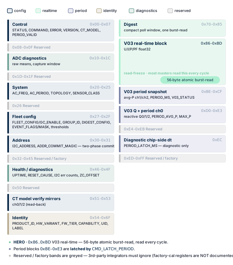
Filter applied: build: production (cal-build registers excluded). Factory-calibration registers (NF, GAIN, PHASE) are not documented — they belong to the factory bench, not the consumer surface.
4.0 Reserved ranges (internal)
The following ranges are reserved for internal/factory use and are not described in this document. Reads return either data that is not relevant to consumer logic or 0x00 for non-existent addresses (see §5.2). Writes to these addresses are either silently dropped or answered with ERR_PARAM:
0x04— internal mode indicator (factory strap, not consumer-settable).0x06,0x26— internal calibration parameters (factory bench).0x08..0x0F— LUT debug view (factory diagnostic).0x1B..0x1F— reserved page-0 (0x18..0x1Aare production diag, see §4.2).0x36..0x45— reserved page-0.0x4F,0x50— reserved (identity-block pre-reserve).0xE4..0xEB,0xF0..0xFF— factory calibration (NF, GAIN); factory-gated writes.
Note on
0xD0..0xE3: in the production build this range is occupied by theV03 Qblock (see §4.12). In the separate cal firmware (not shipped to the consumer) the same range is overlaid with the calibration block (build:cal). The consumer master sees only the production overlay — the Q block.
3rd-party integrators must ignore these ranges.
4.1 Control block (0x00..0x07)
| Addr | Name | Size | Type | Access | Persistence | Notes |
|---|---|---|---|---|---|---|
0x00 |
STATUS |
1 | u8 | r | ram | bit0=READY, bit1=ERROR (mirror of REG_ERROR != 0), bit2=EVENTS_PENDING (mirror of EVENT_FLAGS != 0) |
0x01 |
COMMAND |
1 | u8 | w | ram | Write a CMD_* opcode (see §5.2) |
0x02 |
ERROR |
1 | u8 | r | ram | last-write outcome; 0x00 = OK; 0xFA..0xFF error classes. Clear via CMD_CLEAR_ERROR. See §5.3 |
0x03 |
VERSION |
1 | u8 | r | rom | Protocol version. 0x04 = v1.3 |
0x05 |
CT_MODEL |
1 | u8 | rw | user_config | SCT-013 SKU code (v1.3 pure staging — see §6.2) |
0x07 |
V03_PERIOD_VALID |
1 | u8 | r | ram | Set by CMD_LATCH_PERIOD: 1 = fresh, 0 = empty/stale. NOT cleared-on-read. See §6.3.3 (witness) + §7.5 (failed-latch preservation) |
4.2 ADC diagnostics (0x10..0x1C)
| Addr | Name | Size | Type | Access | Persistence | Notes |
|---|---|---|---|---|---|---|
0x10 |
ADC_MEAN_U |
2 | u16 LE | r | ram | Raw ADC mean U channel (~2048 centered) |
0x12 |
ADC_MEAN_I0 |
2 | u16 LE | r | ram | Raw ADC mean I0 |
0x14 |
ADC_MEAN_I1 |
2 | u16 LE | r | ram | Raw ADC mean I1 (UI2/I2/I3/UI3) |
0x16 |
ADC_MEAN_I2 |
2 | u16 LE | r | ram | Raw ADC mean I2 (UI3/I3) |
0x18 |
CAPTURE_STATUS |
1 | u8 | r | ram | Raw-sample capture: bit0=ready |
0x19 |
CAPTURE_PAGE |
1 | u8 | rw | ram | Page 0..15 → 16 raw I0 samples into CAPTURE_WINDOW |
0x1A |
CAPTURE_WINDOW |
32 | bytes | r | ram | 16×u16 LE pre-LUT I0 codes of the selected page. Burst-read 32 bytes (sized to the 32-byte-max I2C bridge read; no second-half gap). Sweep pages 0..15 for 256 samples total (~1.3 mains periods). Window virtually spans 0x1A..0x39 but only burst-reads from 0x1A are supported. |
0x1D |
LUT_BYPASS |
1 | u8 | rw | ram | Diagnostic: 1 = bypass ADC-INL LUT (identity), 0 = active. For LUT-on/off slope tests. |
4.3 System (0x20..0x25)
| Addr | Name | Size | Type | Access | Persistence | Notes |
|---|---|---|---|---|---|---|
0x20 |
AC_FREQ |
1 | u8 | r | ram | ZC-sourced. 50 or 60 Hz integer. ZC is active on all variants (including I*) |
0x21 |
AC_PERIOD |
2 | u16 LE | r | ram | ⚠ Reads 0 in current firmware — not populated by the zero-cross driver in the v1.4.0 line. Use AC_FREQ (0x20) for mains timing. A fix is planned in the next firmware cycle. |
0x23 |
CALIBRATION |
1 | u8 | r | ram | Legacy calibration status byte |
0x24 |
TOPOLOGY |
1 | u8 | r | rom | 1 = SINGLE, 2 = SPLIT_PHASE, 3 = THREE_PHASE (= N_I) |
0x25 |
SENSOR_CLASS |
1 | u8 | rw | user_config | 0 = UNSET, 1 = SCT_013, 2 = WIRED_CT (resv), 3 = BUILTIN_CT (resv). A class change resets CT_MODEL = 0. Not a variant discriminator (see §3.4) |
4.4 Fleet config (0x27..0x2F)
| Addr | Name | Size | Type | Access | Persistence | Notes |
|---|---|---|---|---|---|---|
0x27 |
FLEET_CONFIG |
1 | u8 | rw | user_config | bit0 = GC_ENABLE (General-Call latch reception; effective after reset). bits 1-7 reserved |
0x28 |
GROUP_ID |
1 | u8 | rw | user_config | GC latch group filter. 0 = respond to all-call. The GC frame group byte must match or be 0x00 |
0x29 |
DIGEST_CONFIG |
1 | u8 | rw | ram | Digest window composition bitmask (see §4.9). Defaults to 0x00 (digest disabled) after reset; rewrite on every initialization |
0x2A |
EVENT_FLAGS |
1 | u8 | w1c | ram | Sticky event bits (see §5.3 error model). Defaults to 0x00 after reset (but bit5 RESET_OCCURRED is set at boot) |
0x2B |
EVENT_MASK |
1 | u8 | rw | ram | Which EVENT_FLAGS bits drive DRDY solid-LOW |
0x2C |
THRESH_I_HI |
2 | u16 LE | rw | ram | Current threshold → EVENT_FLAGS.THRESH_I. Units: 0.01 A. 0xFFFF = disabled |
0x2E |
THRESH_P_HI |
2 | u16 LE | rw | ram | Power threshold → EVENT_FLAGS.THRESH_P. Units: W. 0xFFFF = disabled |
4.5 Address (0x30..0x31)
| Addr | Name | Size | Type | Access | Persistence | Notes |
|---|---|---|---|---|---|---|
0x30 |
I2C_ADDRESS |
1 | u8 | rw | user_config | Two-phase commit: write candidate 0x08..0x77 → RAM staging; arm ADDR_COMMIT_MAGIC; then CMD_COMMIT_ADDR; applies after reset. At boot the active address is read back (v1.3 Fix 4) |
0x31 |
ADDR_COMMIT_MAGIC |
1 | u8 | w | ram | Write 0xA5 to arm CMD_COMMIT_ADDR. Consumed (cleared) on the commit attempt. Reads return 0x00 |
See §6.1 for the sequence.
4.6 Health / diagnostics (0x46..0x4F)
| Addr | Name | Size | Type | Access | Persistence | Notes |
|---|---|---|---|---|---|---|
0x46 |
UPTIME_S |
4 | u32 LE | r | ram | Seconds since boot |
0x4A |
RESET_CAUSE |
1 | u8 | r | ram | Reset reason flags (bit0=PIN, bit1=POR/BOR, bit2=SW, bit3=IWDG, bit4=WWDG, bit5=LPWR) |
0x4B |
I2C_ERR_COUNT |
2 | u16 LE | r | ram | Bus errors (BERR+OVR) since boot, saturating |
0x4D |
I2C_REINIT_COUNT |
1 | u8 | r | ram | I²C peripheral BUSY-recovery reinit count, saturating |
0x4E |
ZC_OFFSET |
2 | u16 LE | r | ram | µs from the last GC-latch STOP edge to the next voltage zero-cross — used for U/I phase compensation in power computation. Firmware-gated to 0xFFFF on I-only variants (no voltage front-end → no voltage ZC). This is not the mains-frequency ZC source — AC_FREQ (0x20) is derived from a dedicated mains-ZC pin and is available on all variants. |
4.7 CT model verify mirrors (0x51..0x53)
Read-only mirrors of the applied CT model preset per channel. The write wire protocol is unchanged (see §6.2) — this is purely a read-back for verification.
| Addr | Name | Size | Type | Access | Persistence | Notes |
|---|---|---|---|---|---|---|
0x51 |
CT_MODEL_CH0 |
1 | u8 | r | user_config | Applied CT model preset on ch0 (verify mirror) |
0x52 |
CT_MODEL_CH1 |
1 | u8 | r | user_config | Applied CT model preset on ch1 |
0x53 |
CT_MODEL_CH2 |
1 | u8 | r | user_config | Applied CT model preset on ch2 |
4.8 Identity (0x54..0x6F)
| Addr | Name | Size | Type | Access | Persistence | Notes |
|---|---|---|---|---|---|---|
0x54 |
PRODUCT_ID |
1 | u8 | r | rom | Family: 0x01 = rbAmp sensor. The master reads this before any family-specific register |
0x55 |
HW_VARIANT |
1 | u8 | r | rom | See §3.1 |
0x56 |
FW_TIER |
1 | u8 | r | rom | bits 0-1: 0=BASIC, 1=STANDARD, 2=PRO; bit 2=bidirectional; bit 3=LUT-calibrated |
0x57 |
CAPABILITY |
2 | u16 LE | r | rom | See §3.2 |
0x59 |
GC_TICK |
2 | u16 LE | r | ram | Master tick from the last accepted GC frame; 0xFFFF = never received |
0x5C |
UID |
12 | bytes | r | rom | 96-bit chip UID. One burst-read. |
0x68 |
LABEL |
8 | bytes | rw | user_config | User location label (ASCII, zero-padded). Empty = unset. Write byte-at-a-time (see §5.1) |
4.9 Digest window (0x70..0x85)
DIGEST is a compact poll window, served by a single burst-read. Its composition is selected by DIGEST_CONFIG (0x29):
DIGEST_CONFIG bit |
Content | Format |
|---|---|---|
| bit 0 | I_RMS[N] |
u16 per channel, 0.01 A |
| bit 1 | U_RMS |
u16, 0.1 V (voltage-HW only) |
| bit 2 | P_REAL[N] |
i16 per channel, 1 W (has_power only) |
| bit 3 | PF[N] |
u8 per channel, 0..100 (has_power only) |
| Addr | Name | Size | Type | Access | Persistence | Notes |
|---|---|---|---|---|---|---|
0x70 |
DIGEST |
22 | bytes | r | ram | Layout: [STATUS_MIRROR u8][SEQ u8] + mask-enabled fields. The maximum payload (UI3 full mask) is 19 B + 2 B header = 21 B used; 1 B tail unused (reads 0x00). SEQ increments per RT commit, wrapping 255→0. Atomic via read-freeze (see §5.4). |
Layout is dynamic per DIGEST_CONFIG — each enabled bit appends its fields in a fixed order: I_RMS[N] → U_RMS → P[N] → PF[N]. Disabled bits leave no padding — fields slide forward. The master must parse with the same mask it wrote into DIGEST_CONFIG. A burst-read of 22 bytes is safe (the tail is 0x00 whenever the total payload is < 22 bytes). The single-byte tail is always 0x00 (reserved).
4.10 V03 real-time block (0x86..0xBD)
All float32 LE (IEEE 754 single precision, standard little-endian byte order). The byte-for-byte layout is frozen at v1.2. Every register is r access, ram persistence, group v03_rt. Atomic via read-freeze (see §5.4): a 56-byte burst-read (0x86..0xBD) is guaranteed contiguous (no torn snapshot).
| Addr | Name | Size | Type | Access | Persistence | Units | Notes |
|---|---|---|---|---|---|---|---|
0x86 |
V03_U_RMS |
4 | float32 LE | r | ram | V | 0.0 on I-variants |
0x8A |
V03_U_PEAK |
4 | float32 LE | r | ram | V | |
0x8E |
V03_I0_RMS |
4 | float32 LE | r | ram | A | |
0x92 |
V03_I1_RMS |
4 | float32 LE | r | ram | A | 0.0 if the variant lacks ch1 |
0x96 |
V03_I2_RMS |
4 | float32 LE | r | ram | A | 0.0 if the variant lacks ch2 |
| ⛔ | STOP — flat per-channel RMS ends at channel 2. | The next row (0x9A) is V03_I0_PEAK, NOT V03_I3_RMS. Do NOT extrapolate the step-4 pattern past channel 2 — you will read plausible but silently wrong numbers (peak, not RMS; ch0, not ch3). Channels 3+ (UI5/UI7) are accessed only through the Channel access window — see §4.14. |
|||||
0x9A |
V03_I0_PEAK |
4 | float32 LE | r | ram | A | |
0x9E |
V03_I1_PEAK |
4 | float32 LE | r | ram | A | |
0xA2 |
V03_I2_PEAK |
4 | float32 LE | r | ram | A | |
0xA6 |
V03_P0_REAL |
4 | float32 LE | r | ram | W | 0.0 on I-variants (no power calc) |
0xAA |
V03_P1_REAL |
4 | float32 LE | r | ram | W | |
0xAE |
V03_P2_REAL |
4 | float32 LE | r | ram | W | |
0xB2 |
V03_PF0 |
4 | float32 LE | r | ram | – | range −1..+1 |
0xB6 |
V03_PF1 |
4 | float32 LE | r | ram | – | |
0xBA |
V03_PF2 |
4 | float32 LE | r | ram | – |
4.11 V03 period block (0xBE..0xCF)
A period snapshot latched on CMD_LATCH_PERIOD. Ragged layout (historical legacy from v1.2, frozen at v1.3): avg_p for ch1/ch2 lives here, while avg_p for ch0 sits in §4.12 at address 0xDC (the legacy energy primitive was not relocated, to avoid an API break for existing integrators). Logically these three values belong to the same group.
| Addr | Name | Size | Type | Access | Persistence | Units | Notes |
|---|---|---|---|---|---|---|---|
0xBE |
V03_PERIOD_COMMIT_CNT |
4 | u32 LE | r | ram | – | RT commits in the current period (diagnostic) |
0xC2 |
V03_PERIOD_AVG_P_CH1 |
4 | float32 LE | r | ram | W | Latched avg P ch1 (UI2 only; UI3 — roadmap) |
0xC6 |
V03_PERIOD_AVG_P_CH2 |
4 | float32 LE | r | ram | W | Latched avg P ch2 (UI3 only — roadmap) |
0xCA |
V03_PERIOD_MS |
4 | u32 LE | r | ram | ms | Current period duration |
0xCE |
V03_STATUS |
1 | u8 | r | ram | – | bit 0 = valid (RT commit outcome). NOT cleared-on-read. The master polls STATUS (0x00) for ready-wait. Alias DATA_VALID is sometimes used for this register in tutorial chapters — same address, same semantics. |
4.12 V03 Q + period ch0 (0xD0..0xE3, production build)
| Addr | Name | Size | Type | Access | Persistence | Units | Notes |
|---|---|---|---|---|---|---|---|
0xD0 |
V03_Q0_REAC |
4 | float32 LE | r | ram | VAr | Reactive power ch0 (IEEE 1459 quadrature) |
0xD4 |
V03_Q1_REAC |
4 | float32 LE | r | ram | VAr | |
0xD8 |
V03_Q2_REAC |
4 | float32 LE | r | ram | VAr | |
0xDC |
V03_PERIOD_AVG_P |
4 | float32 LE | r | ram | W | PRODUCTION energy primitive: latched avg P ch0, ≥ 0 (BASIC unidirectional clamp). Logically grouped with V03_PERIOD_AVG_P_CH1/CH2 (§4.11); the legacy layout is preserved for compatibility |
0xE0 |
V03_PERIOD_MAX_P |
4 | float32 LE | r | ram | W | Latched max P ch0 this period |
4.13 Diagnostic chip-side dt (0xEC)
| Addr | Name | Size | Type | Access | Persistence | Units | Notes |
|---|---|---|---|---|---|---|---|
0xEC |
V03_PERIOD_LATCH_MS |
4 | u32 LE | r | ram | ms | Chip-side dt between the two most recent latches. DIAGNOSTIC-ONLY — undercounts by 25–30% under load (SysTick starvation, by design). DO NOT use for billing — the master keeps its own wall-clock. See §7.4 |
4.14 Channel access window (0x32 + 0x3C..0x3F)
Applies to UI5 (5-channel) and UI7 (7-channel) modules. On UI1/UI2/UI3 and I1/I2/I3 it is available too — a single unified path if you prefer it over §4.10 flat registers.
Channels 3..6 have no flat per-channel registers (there was room for 8 bytes in the 8-bit address space, and a flat layout would need ~88). Instead a select-and-read window is exposed:
| Addr | Name | Size | Type | Access | Persistence | Notes |
|---|---|---|---|---|---|---|
0x32 |
REG_CHANNEL_SELECT |
1 | u8 | rw | ram | This is a register address, NOT the command opcode CMD_SAVE_USER_CONFIG — they collide numerically. Always cite 0x32 with the register-vs-command space you mean. Encoded as (field << 4) \| channel. channel nibble range is 0..15 (reserved for up to 16 channels); the physical maximum per SKU is channels() (7 on UI7). Writes to a channel index >= channels() are silently discarded (no ERR_PARAM). field per table below. Writing the selector snapshots the requested value into REG_CHANNEL_DATA. |
0x3C..0x3F |
REG_CHANNEL_DATA |
4 | float32 LE (u16 LE for NF) | r | ram | Data buffer for the selection. float32 LE for all public fields; NF returns u16 LE zero-padded to 4 bytes. |
Field codes (nibble high in 0x32):
| Code | Field | Type | Access | Meaning |
|---|---|---|---|---|
0 |
CHFIELD_I_RMS |
float32 LE | r | Live RMS current for the selected channel (units A) |
1 |
CHFIELD_I_PEAK |
float32 LE | r | Live peak current (units A) |
2 |
CHFIELD_P_REAL |
float32 LE | r | Live real power (units W) |
3 |
CHFIELD_PF |
float32 LE | r | Live power factor (−1..+1) |
4 |
CHFIELD_NF |
u16 LE (zero-padded to 4) | rw | Noise floor (calibration) |
5 |
CHFIELD_GAIN |
float32 LE | rw | Channel gain (calibration) |
6..12 |
(reserved — private diagnostics) | – | – | Not documented for user code; do not depend on values or codes. |
13 |
CHFIELD_PERIOD_AVG_P |
float32 LE | r | Latched period-average real power (W). For channels 3+ this is the ONLY period/energy field — flat V03_PERIOD_AVG_P* (§4.11/§4.12) only covers ch0..ch2. |
14 |
(reserved) | – | – | Reserved for future firmware; do not depend on. |
15 |
CHFIELD_CT_MODEL |
u8 in 0x3C (bytes 0x3D..0x3F read as zero-padding) |
rw | Firmware ≥ v1.4.18-24M. Per-channel CT model code for the selected channel (0..N-1). Read returns the applied model on the channel. Write is RAM-only and applies immediately: GAIN/NF for that channel are switched to the preset values in the same transaction; no separate commit command, no CMD_SET_CT_MODEL_CH* needed. Writes are byte-at-a-time per the wire-protocol rule (§5.1). An unknown (SENSOR_CLASS, code) pair returns ERR_PARAM (0xFE) and the channel keeps its previous model — no partial state. Senior-SKU channels (ch3+) NO LONGER inherit the global model — each channel must be configured explicitly via field 15. Persistence: CMD_SAVE_USER_CONFIG (opcode 0x32 on REG_COMMAND, ungated) persists all channels' models to the user-config flash page in one command. A write without a subsequent CMD_SAVE_USER_CONFIG reverts on reboot. The set of accepted (class, code) pairs is defined by the canonical model registry (sensor_models.yaml); a code that shipped in your firmware version is authoritatively confirmed by the module — write it, read it back, and check REG_ERROR. On modules running v1.4.0 (BATCH001/BATCH002 shipped) writing this field returns ERR_PARAM; use per-channel commands + flat REG_CT_MODEL staging instead. |
The four traps — read this before writing code
- ⛔ Flat per-channel RMS ends at channel 2. The rows
V03_I0_RMS(0x8E) →V03_I1_RMS(0x92) →V03_I2_RMS(0x96) are step-4, and0x9Acontinues the step — but0x9AisV03_I0_PEAK, notV03_I3_RMS. Extrapolating the pattern silently returns peak-of-ch0 instead of RMS-of-ch3. Firmware cannot detect the mistake; the value looks plausible. Channels 3+ live only in the channel access window. - Re-select before every read.
REG_CHANNEL_DATAis a snapshot taken at the moment of the selector write, not a live view. Polling0x3C..0x3Fin a loop without re-writing0x32returns a frozen value forever. Every fresh reading requires a fresh write to0x32. 0x32register address ≠0x32command opcode.CMD_SAVE_USER_CONFIGuses opcode0x32written toREG_COMMAND(0x30) — that is a different address space thanREG_CHANNEL_SELECT(which sits at register address0x32). Never quote0x32without saying which space.- For channels 3+ period/energy comes only from field
13(CHFIELD_PERIOD_AVG_P). RegistersV03_PERIOD_AVG_P*(0xC2/0xC6/0xDC) only cover ch0/ch1/ch2. There is no flatV03_PERIOD_AVG_P_CH3— read field 13 via the window instead.
Wire-level example — read RMS current for channel 3
# select field=0 (I_RMS), channel=3  →  (0 << 4) | 3  =  0x03
write_u8(REG_CHANNEL_SELECT=0x32, 0x03)
# read 4 bytes at REG_CHANNEL_DATA — float32 LE
bytes = read(0x3C, 4)
i3_rms = unpack_float32_le(bytes)   # amperes
For channel 4 peak current: selector = (1 << 4) | 4 = 0x14, then read 0x3C..0x3F. For channel 5 period-average power: selector = (13 << 4) | 5 = 0xD5, then read 0x3C..0x3F.
Wire-level example — read RMS current on ALL channels of a UI7 module
Combines both paths in one loop: flat RT block for ch 0..2, channel access window for ch 3..6.
# --- Discover physical channel count -----------------------------
N = read_u8(TOPOLOGY=0x24)      # 5 on UI5, 7 on UI7
# --- ch 0..2 via flat block (single 12-byte burst) ---------------
bytes = read(V03_I0_RMS=0x8E, 12)
i0 = unpack_float32_le(bytes[0:4])
i1 = unpack_float32_le(bytes[4:8])
i2 = unpack_float32_le(bytes[8:12])
# --- ch 3..N-1 via channel access window (re-select per read) ----
i_rms = [i0, i1, i2]
for ch in range(3, N):
    write_u8(REG_CHANNEL_SELECT=0x32, (0 << 4) | ch)   # field 0 = I_RMS
    i_rms.append(unpack_float32_le(read(REG_CHANNEL_DATA=0x3C, 4)))
# i_rms is now length-N: RMS current for every physical channel of the module.
The same pattern extends to I_PEAK (field 1), P_REAL (field 2), PF (field 3), and the latched PERIOD_AVG_P (field 13) — flat block for ch0..ch2, window for ch3+. Field 13 is the ONLY period/energy source for ch3+ — the flat block has no V03_PERIOD_AVG_P_CH3..6.
For per-channel CT model configuration on any channel (0..N-1), use window field 15 (CHFIELD_CT_MODEL): write (15 << 4) | ch to 0x32, then write the model code as one byte to 0x3C. Persist all channels' models with a single CMD_SAVE_USER_CONFIG (opcode 0x32 on REG_COMMAND (0x30) — ungated).
Recommendation for new integrations
The window covers channels 0..6 — you can use it as a single unified path for all channels instead of branching between flat registers (ch0..ch2) and window (ch3..ch6). For fleets that mix junior (UI1/UI2/UI3) and senior (UI5/UI7) SKUs this eliminates a code split. Latency is one extra small write per reading (compared to a straight burst-read of the flat block).
5 · Wire protocol
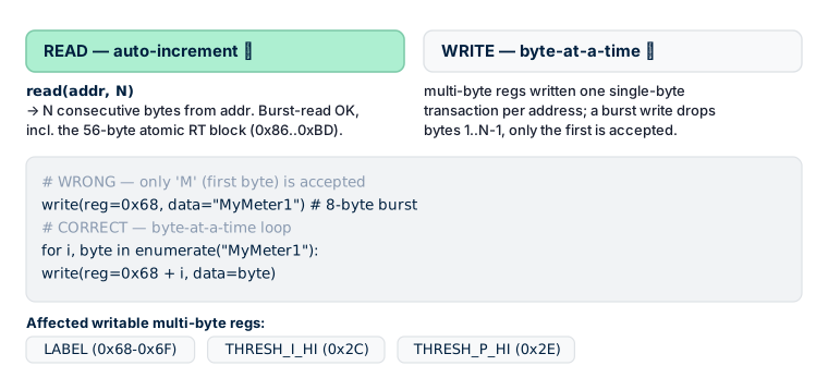
5.1 READ / WRITE asymmetry
Canonical by-design behavior:
| Direction | Auto-increment | Pattern |
|---|---|---|
| READ (burst-read N bytes) | ✅ YES | read(addr, N) returns N consecutive bytes starting at addr. |
| WRITE (multi-byte regs) | ❌ NO | A multi-byte register is written byte-at-a-time — one separate single-byte transaction per address. A burst write drops bytes 1..N-1 and only accepts the first. |
Affected writable multi-byte registers (write byte-at-a-time)
LABEL(0x68-0x6F, 8 bytes)THRESH_I_HI(0x2C, 2 bytes u16 LE)THRESH_P_HI(0x2E, 2 bytes u16 LE)
Endianness for multi-byte WRITE: the byte at the lower address is the low byte (LE). For example, to write THRESH_I_HI = 0x1234 (4660 decimal):
# CORRECT: low byte first (LE)
write(addr=0x2C, value=0x34)   # LO byte
write(addr=0x2D, value=0x12)   # HI byte
WRONG / CORRECT example (pseudocode)
# WRONG — only 'M' (first byte) is accepted, the rest are dropped
write(addr=0x50, reg=0x68, data=b"MyMeter1")   # 8-byte burst
# CORRECT — byte-at-a-time loop
label = b"MyMeter1"
for i, byte in enumerate(label):
    write(addr=0x50, reg=0x68 + i, data=byte)
Exception — GC broadcast frame
The GC broadcast frame (0x00 general-call address + 5-byte payload) is a separate wire-protocol path, not a register write. The read/write asymmetry from §5.1 does not apply to GC. See §6.3.
5.2 Unmapped registers behavior
Any read from an unmapped address returns 0x00. The firmware never NACKs on register reads. This is by design (wedge fix).
Implication for detection: detection of a missing device must go through the I²C address-frame ACK, not through register probes.
5.3 Error model
v1.3 canonical:
REG_ERROR (0x02)is the last-write outcome, NOT sticky. On every register write the firmware setsreg_error = ERR_OK; any subsequent unrelated write clears the prior error.EVENT_FLAGS (0x2A) bit 3is the durable signal (sticky W1C), asserted on any rejected write or command.
Error codes
| Code | Name | Severity |
|---|---|---|
0x00 |
OK | – |
0xF9 |
CLONE |
reserved (anti-clone sentinel — ⚠ NOT raised by v1.4.x firmware; the anti-clone verification is not implemented in shipped modules. Code is reserved for a future firmware cycle) |
0xFA |
LUT_BAD |
error |
0xFB |
FLASH_PARAMS_BAD |
error (see §6.5 fresh-flash) |
0xFC |
NOT_READY |
error |
0xFD |
SENSOR_OVERFLOW |
error |
0xFE |
PARAM |
error (rejected write — invalid arg / unknown opcode / out-of-range enum) |
0xFF |
UNHANDLED |
error |
EVENT_FLAGS (0x2A) layout (sticky W1C)
| bit | Name | Notes |
|---|---|---|
| 0 | PERIOD_READY |
latch snapshot available |
| 1 | THRESH_I |
I_rms crossed THRESH_I_HI |
| 2 | THRESH_P |
P sum crossed THRESH_P_HI |
| 3 | ERROR |
REG_ERROR != 0 (durable error signal) |
| 4 | CONFIG_CHANGED |
class/model/address/label modified |
| 5 | RESET_OCCURRED |
module rebooted (set at boot until W1C). The master must re-initialize RAM config. |
Canonical error patterns
Pattern 1 — one-off post-operation capture (outcome of exactly that operation):
write target_reg(...)
err = read_u8(0x02)   # IMMEDIATELY after the operation, before the next write
Pattern 2 — durable monitoring (canonical for a long-running master):
event_flags = read_u8(0x2A)
if event_flags & (1 << 3):    # ERROR bit
    last_err = read_u8(0x02)
    # handle
    write_u8(0x2A, 1 << 3)    # W1C clear bit 3
    # or CMD_CLEAR_ERROR
⚠ bit 3 async caveat
A write rejection asserts EVENT_FLAGS.bit3 asynchronously, ~200 ms after the operation, not immediately. Do not poll bit 3 right after a write — either wait ≥ 200 ms, or use Pattern 1 (immediate REG_ERROR capture) for the outcome of a specific operation, and reserve bit 3 polling for long-running monitoring.
Anti-clone sentinel
⚠ Not implemented in v1.4.x firmware. The anti-clone verification described in this section is a planned mechanism (
CMD_SEAL0x33 to provision a UID-seal signature, plus a boot-time verify step raisingDEV_ERR_CLONE 0xF9). Shipped modules on the v1.4.0 line do NOT compute the seal and do NOT run the check —DEV_ERR_CLONE (0xF9)is never raised by current firmware. The description below applies when the mechanism ships. This documentation is retained for forward-compatibility and will be updated in the release notes when the mechanism lands.
DEV_ERR_CLONE (0xF9) is not cleared by CMD_CLEAR_ERROR or by W1C bit 3. Only a reboot plus a factory reset can clear it (intentional anti-clone protection).
5.4 Atomicity / read-freeze semantics
5.4.1 Read-freeze present (atomic — NOT torn)
These blocks are protected by firmware-side read-freeze. A burst-read is atomic with respect to the RT commit:
- V03 RMS / P / PF block (0x86..0xBD) — the full float block.
- Digest block (0x70..0x85).
Burst-reads of these ranges are safe — there is no split sample between two consecutive commits.
5.4.2 No read-freeze — read-twice-agree recommended
These registers are updated asynchronously without within-read freeze. Single-byte reads are tolerant, but the value can change between transactions:
GC_TICK (0x59)— GC tick counter.I2C_ADDRESS (0x30)— RAM staging mirror.CT_MODEL_CH0/1/2 (0x51..0x53)— verify mirrors.
Pattern for reliable reads:
val1 = read_u8(addr)
val2 = read_u8(addr)
if val1 == val2:
    return val1   # stable
else:
    retry          # value changed between reads
5.4.3 NF-clamp semantics
I_RMS = 0x00000000 means "signal below noise floor" (the firmware computes rms_corr² = max(0, raw² − nf²)), NOT "no data" / "error". It is a valid measurement for no-load / very-low-load scenarios.
The master code must not interpret I_RMS = 0.0 as an error or missing data.
6 · Protocol sequences
6.0 Cold-boot timeline
After POR (power-on reset) or hard reset the module passes through the following phases:
| Time from POR | State |
|---|---|
| 0 ms | POR — all registers in reset state, SCL/SDA tri-stated |
| ~10 ms | Bus-responsive (the module ACKs its address) |
| ~50 ms | First RT commit (the RT block at 0x86+ holds valid data; STATUS.bit0 = 1) |
| ~60-80 ms | First valid V03_STATUS.bit0 (RT pipeline has cycled through one full mains period) |
| ~200 ms | First CMD_LATCH_PERIOD may return V03_PERIOD_VALID = 1 (latch requires ≥ 1 mains period of accumulation) |
| ~250 ms | All measurements stable (typical) |
Holistic cold boot to the first valid measurement ≈ 250 ms (typical). After a soft
CMD_RESETthe timeline is identical (the full reset state machine runs).
Master initialization sequence:
1. wait ~50 ms after VCC stable
2. probe slave address (read PRODUCT_ID = 0x54); retry up to 300 ms on NACK
3. read identity (HW_VARIANT 0x55, CAPABILITY 0x57/0x58); validate
4. check REG_ERROR (0x02):
   - 0x00 — normal boot
   - 0xFB — fresh flash, provisioning required (§6.5)
   - other — see §6.7 error-state recovery
5. configure (SENSOR_CLASS, CT_MODEL, FLEET_CONFIG, etc.)
6. poll STATUS (0x00) until bit0 = 1 (READY) — usually immediate after step 5
6.1 Address change — two-phase commit (production-OK)
Wire protocol (v1.3 canonical):
1. write candidate_addr (1 byte) → REG_I2C_ADDRESS (0x30)   # RAM staging, not persisted
2. write 0xA5 → REG_ADDR_COMMIT_MAGIC (0x31)                # arm commit
3. issue CMD_COMMIT_ADDR (opcode 0x30 in REG_COMMAND)        # persists into flash
4. wait ~700 ms (flash write completion; see §6.6 settle)
5. issue CMD_RESET (opcode 0x01)                             # module resets
6. wait ~300 ms boot-to-responsive
7. verify: bus-probe the new address (ACK = success)Note:
CMD_COMMIT_ADDRdoes NOT auto-reset the module — an explicitCMD_RESETis required at step 5. If the master skips the explicit reset, the new address remains stored in flash, but the old address stays active until the next external reset (power cycle, hard reset pin, IWDG).
Guarantees:
- Address change works in production mode (not factory-only).
REG_I2C_ADDRESS (0x30)at boot reads the active address (v1.3 canonical). Until reboot after staging it echoes the candidate.- The address is excluded from the
CMD_SAVE_GAINS/CMD_SAVE_USER_CONFIGnamespace — it is persisted only throughCMD_COMMIT_ADDR.
Boot-window timing for verification:
- Minimum 300 ms boot-to-responsive.
- Retry window on the new address: ~1 s total (if a NACK persists after 1-2 retries, an additional boot delay may be needed).
- Once the new address ACKs, optionally verify by reading 0x30 (which now reflects the new active address) for confirmation.
Failure modes:
ADDR_COMMIT_MAGICnot armed →CMD_COMMIT_ADDR→REG_ERROR = ERR_PARAM (0xFE).- Candidate out of range (< 0x08 or > 0x77) →
ERR_PARAM. - 5 s timeout without commit → magic clears; the
preparestep must be repeated.
6.2 CT model binding — pure staging + per-channel CMD
v1.3 pure-staging canonical: writing REG_CT_MODEL (0x05) no longer auto-applies the preset to ch0. Binding happens only through CMD_SET_CT_MODEL_CHn.
Canonical per-channel wire protocol (order-independent in v1.3):
1. write REG_SENSOR_CLASS (0x25) = sct013    # if not already set
2. write REG_CT_MODEL (0x05) = model_code     # stages, applies nothing
3. issue CMD_SET_CT_MODEL_CHn (opcode 0x28/0x29/0x2A for ch0/1/2)
   # VALIDATES (class, model) + binds to channel n
4. wait 5 ms settle
5. (optional) issue CMD_SAVE_USER_CONFIG (opcode 0x32) for persistenceOrder-independent: in v1.3 channels may be configured in any order — ch0 first, last, whatever is convenient. The "bind ch0 last" workaround from v1.2 is no longer required.
Read-back verification: after binding, read CT_MODEL_CH0/1/2 (0x51..0x53) — those reflect the applied state per channel.
Failure modes (validation of (class, model) happens at the CMD_SET_CT_MODEL_CHn bind step, not at the pure-staging write to 0x05):
- SENSOR_CLASS = 0 (UNSET) when CMD_SET_CT_MODEL_CHn is issued → REG_ERROR = ERR_PARAM.
- CT_MODEL outside 1..7 (SCT-013-005/-010/-030/-050/-100/-020/-060) at CMD_SET → ERR_PARAM.
6.3 GC broadcast latch — opt-in fleet sync
Opt-in per module via REG_FLEET_CONFIG.bit0 (GC_ENABLE). Default OFF. The change is effective after reset (soft CMD_RESET or hard reset).
6.3.1 Enable sequence (once per module)
1. write REG_FLEET_CONFIG (0x27) = 0x01    # bit0 = GC_ENABLE
2. issue CMD_SAVE_USER_CONFIG (opcode 0x32, ungated)
3. issue CMD_RESET (opcode 0x01)
4. wait ~300 ms boot
5. verify: read REG_FLEET_CONFIG → bit 0 should be 1
6.3.2 GC frame format
I²C general-call address 0x00 | A5 27 <group> <tick_lo> <tick_hi> (5-byte payload)A5— frame magic.27— opcodeCMD_LATCH_PERIOD.<group>—0x00= all-call; otherwise must match the device'sREG_GROUP_ID (0x28).<tick_lo/hi>— 16-bit master-side tick counter (for fleet-wide window numbering and per-module missed-frame detection viaGC_TICK (0x59)).
Latch-only: GC frames do not carry destructive opcodes (SAVE_*, COMMIT_ADDR, FACTORY_RESET, etc.) by design.
6.3.3 Failure mode detection — 2-level
Level 1 — GC-address NACK (immediate, at bus level):
- If GC is disabled across the entire fleet → the master receives a hard error (NACK on address 0x00, or the driver-side equivalent).
- This is a hard error, NOT a silent drop — the master can detect and react.
- Trip: NACK on GC = "GC is not enabled on any device in the fleet."
Level 2 — per-module witness (after settle):
- If no NACK occurs (at least one module is listening), the master reads REG_V03_PERIOD_VALID (0x07) from every expected slave.
- 1 = the latch succeeded on that module.
- 0 = GC is disabled on that specific module, or the current period is empty.
Fall back to per-device latch if the witness reports 0:
foreach module where witness == 0:
    write_cmd(module, CMD_LATCH_PERIOD)
sleep(50 ms)
foreach module: read period snapshot with skip_latch=true
6.4 Period sync — two strategies
Strategy 1 — sequential latch + shared settle (any firmware)
for module in modules:
    write_cmd(module, CMD_LATCH_PERIOD)
sleep(50 ms)
for module in modules:
    read_period_snapshot(module)   # skip_latch=true
Skew between modules: ~1 ms per module at 50 kHz. Over 16 modules relative to a 60-second period that is 0.027 %. Negligible for billing.
Settle window after CMD_LATCH_PERIOD:
- Minimum 50 ms before reading V03_PERIOD_VALID (0x07) or the period snapshot — this covers worst-case latch latency (1 mains period @ 50 Hz = 20 ms + RT commit + I²C peripheral settling).
- Optionally the master can poll STATUS.bit0 (READY) instead of a fixed sleep: READY=1 means the RT block is in a consistent state, so the period snapshot can be safely burst-read.
- On a brand-new module (< 200 ms after boot) a latch may return V03_PERIOD_VALID = 0 because less than 1 mains period has accumulated — see §6.0 cold-boot timeline.
Strategy 2 — General-Call broadcast latch (enable required)
Skew = 0 (atomic at bus level). See §6.3.
When to use what: - < 8 modules: Strategy 1 (simpler, no enable required). - ≥ 8 modules or billing-grade synchrony: Strategy 2.
6.5 Provisioning — fresh-flash + SAVE
Freshly flashed module behavior:
- On the first boot after firmware flash:
REG_ERROR = 0xFB (FLASH_PARAMS_BAD)+EVENT_FLAGS.bit3set. - The params page is uninitialized → factory defaults are loaded.
This is NORMAL for a virgin module and not fatal. Do not abort provisioning on first-boot 0xFB.
Recovery:
1. configure SENSOR_CLASS + CT_MODEL (per §6.2)
2. (optional) configure FLEET_CONFIG + GROUP_ID + LABEL
3. issue CMD_SAVE_USER_CONFIG (opcode 0x32, ungated)
4. wait ~700 ms (flash write)
5. verify: REG_ERROR = 0x00, EVENT_FLAGS.bit3 cleared
6.7 Error-state recovery — decision tree
If at boot or runtime STATUS.bit1 (ERROR) = 1 or the durable signal EVENT_FLAGS.bit3 (ERROR) is set, the master reads REG_ERROR (0x02) and decides based on the code:
read REG_ERROR (0x02):
  0x00  → no error (false signal — clear stale EVENT bit3 via W1C)
         action: write 1<<3 → EVENT_FLAGS (W1C clear)
  0xF9  → CLONE (anti-clone sentinel — RESERVED, NOT raised by v1.4.x)
         action: not reachable in current firmware — the anti-clone
                 mechanism is planned but not implemented. If ever raised
                 by a future firmware version: device unusable; measurement
                 pipeline halted. Only STATUS/ERROR readable. NOT clearable
                 through software. Resolution — factory recovery.
  0xFA  → LUT_BAD (calibration LUT corrupted)
         action: device unusable for measurement. Factory recovery required.
  0xFB  → FLASH_PARAMS_BAD (params page uninitialized — virgin module)
         action: NORMAL for a freshly flashed module. Provision per §6.5
                 (configure SENSOR_CLASS/CT_MODEL/...; issue CMD_SAVE_USER_CONFIG).
                 Cleared after a successful SAVE.
  0xFC  → NOT_READY (transient; module still booting)
         action: wait 50 ms, retry. If persistent > 300 ms — power cycle.
  0xFD  → SENSOR_OVERFLOW (transient; signal saturated)
         action: physical overload detected. The chosen CT clamp has
                 insufficient range for the measured current, or a real overload.
                 Issue CMD_CLEAR_ERROR (0x31) after the cause is removed.
  0xFE  → PARAM (last operation rejected — invalid argument / unknown opcode)
         action: master-side bug — review the last write. Issue CMD_CLEAR_ERROR
                 after fixing the master logic.
  0xFF  → UNHANDLED (firmware-side anomaly)
         action: open an issue with the vendor; CMD_CLEAR_ERROR attempts to clear.
                 If persistent after CMD_RESET — the device is suspect.
General recovery flow for transient errors (0xFC/0xFD/0xFE):
1. capture context (what was the last write? master state?)
2. issue CMD_CLEAR_ERROR (opcode 0x31)
3. wait 5 ms
4. re-read STATUS / REG_ERROR — verify cleared
For persistent errors — issue CMD_RESET and walk through the cold-boot timeline (§6.0). If the error persists after reset and is not 0xFB (fresh-flash) — contact vendor support.
6.6 Commands reference
Core opcodes (write to REG_COMMAND (0x01))
| Opcode | Name | Settle | Gated | Notes |
|---|---|---|---|---|
0x01 |
RESET |
~300 ms | – | Soft reset (HAL_NVIC_SystemReset) |
0x27 |
LATCH_PERIOD |
50 ms | – | Latch RT counters into the period snapshot |
0x28 |
SET_CT_MODEL_CH0 |
5 ms | – | Bind staged REG_CT_MODEL to ch0 |
0x29 |
SET_CT_MODEL_CH1 |
5 ms | – | Bind staged REG_CT_MODEL to ch1 |
0x2A |
SET_CT_MODEL_CH2 |
5 ms | – | Bind staged REG_CT_MODEL to ch2 |
0x30 |
COMMIT_ADDR |
700 ms | – | Persist I2C_ADDRESS (see §6.1) |
0x31 |
CLEAR_ERROR |
0 | – | Clear REG_ERROR (transient classes only; CLONE is not clearable) |
0x32 |
SAVE_USER_CONFIG |
700 ms | – | Persist the user_config group (production-OK) |
Opcodes outside the public range (factory-only) are not documented in this reference. A consumer master does not send them in normal operation; an unsupported opcode →
REG_ERROR = ERR_PARAM (0xFE).
7 · Semantics
7.0 Flash endurance + reset behavior
Flash endurance: ~10 000 cycles per page (typical, vendor spec). Every CMD_SAVE_USER_CONFIG or CMD_COMMIT_ADDR is one erase+write cycle on the params page.
⚠ Do not loop SAVE/COMMIT in a runtime loop. At 1 SAVE/s a module burns out in about 3 hours. Provisioning is done once at install time; no runtime setting updates are required (a consumer master rarely changes them).
Retention: typically 10+ years at typical operating temperature.
Reset behavior comparison:
| Reset type | Preserved | Cleared |
|---|---|---|
CMD_RESET (0x01) |
flash (config, address, label, gains, NF) | RAM (UPTIME, ZC_OFFSET, EVENT_FLAGS — except RESET_OCCURRED bit 5 set at boot; THRESH_*; DIGEST_CONFIG) |
| Power cycle / hard reset pin | flash | same as CMD_RESET plus any external RAM held on the host side |
CMD_FACTORY_RESET (0xAA) (factory mode only) |
nothing | everything — wipes flash + RAM (full factory reset) |
Note: factory mode = provisioning state set at manufacture (not user-accessible); factory reset = a command that restores defaults (production-OK).
RESET_OCCURRED bit pattern (canonical):
- After a reset, on boot: EVENT_FLAGS.bit5 = 1.
- The master sees bit 5 → knows the module rebooted → must re-initialize the RAM-only fields (DIGEST_CONFIG, THRESH_*, EVENT_MASK).
- The master clears bit 5 via W1C: write 1<<5 → EVENT_FLAGS.
7.1 Persistence model
| Command | Production | Persists |
|---|---|---|
CMD_SAVE_USER_CONFIG (0x32) |
✅ OK | i2c_address (via two-phase), ct_model, sensor_class, fleet_config, group_id, label |
CMD_COMMIT_ADDR (0x30) |
✅ OK (magic-armed) | i2c_address |
CMD_RESET (0x01) |
✅ OK | — (soft reset) |
CMD_LATCH_PERIOD (0x27) |
✅ OK | — (latches the period snapshot) |
CMD_CLEAR_ERROR (0x31) |
✅ OK | — (clears REG_ERROR) |
CMD_SAVE_GAINS (0x26) |
❌ BLOCKED in production (silent reject; REG_ERROR = 0xFE; reboot reverts) |
factory calibration |
CMD_FACTORY_RESET (0xAA) |
❌ BLOCKED in production | — |
7.2 Read-back ≠ persistence
⚠ The production guard accepts the write into RAM (a subsequent read returns the written value), but the flash save may be rejected. After reboot the value reverts to its pre-write state.
The only valid way to confirm persistence is CMD_RESET + boot-wait + re-read:
1. write target_reg(...)
2. issue CMD_RESET (0x01)
3. wait ~300 ms boot
4. re-read target_reg
5. assert read == written     # only now is persistence confirmed
Address is an exception (v1.3 canonical): REG_I2C_ADDRESS (0x30) at boot reads the active address. After staging it echoes the candidate; after reboot it shows the actual persisted value.
7.3 Single voltage reference caveat
The module uses one U channel to compute P on all I channels. If a CT clamp hangs on a wire of another phase (multi-phase distribution panel) — the P readings for that channel will be wrong (arbitrary U/I phase offset). I_RMS remains correct.
Multi-phase measurement (L1/L2/L3 simultaneously) is a separate SKU with its own specification.
7.4 Master energy integration — wall-clock canon
⚠ V03_PERIOD_LATCH_MS (0xEC) is a diagnostic-only chip-side software timer (SysTick-based). It undercounts by 25–30% under normal ISR load (SysTick starvation, by design). DO NOT use for billing.
Canonical master energy integration:
# CORRECT — master wall-clock
t_now = master_clock()
dt_s = (t_now - t_prev_latch) / time_unit
energy_wh[ch] += avg_p[ch] * dt_s / 3600
t_prev_latch = t_now
# WRONG — chip software timer undercounts by 25-30%
dt_chip_s = read_u32(0xEC) / 1000.0
energy_wh[ch] += avg_p[ch] * dt_chip_s / 3600    # systematically under-reported
7.5 Failed-latch period preservation
The firmware PRESERVES the period accumulator on an empty latch. When g_period_count == 0 (a latch with no readable period):
- REG_V03_PERIOD_VALID = 0 (signal stale).
- period_start_ms is preserved → the next successful latch covers the full master-intended interval.
Implication: the master does not lose data on a stale latch. Pattern for master integration:
issue latch
if PERIOD_VALID == 1:
    integrate(avg_p, master_dt)
    reset_master_clock
# else: skip integration (FW will automatically recover on the next success)
7.6 Clock-drift tolerance
Canon: chip-timebase drift up to 30 % under load is normal (SysTick starvation, by design on this MCU/ISR profile). Hardware-measured under production ISR load.
Acceptance: the chip is OK at drift ≤ 30 %.
⚠ The legacy 3 % threshold is WRONG. That threshold would mass-reject healthy chips.
7.7 EMI / switch-transient resilience
Reads during active relay switching (5 A EMI) fail ~67 % of the time (HW-measured). Steady-state reads are reliable. The bus self-recovers, no wedge occurs, no modules are lost.
Master pattern — application-level retry (mandatory when switching inductive loads):
for attempt in range(5):
    result = read_register(...)
    if result is OK:
        return result
    sleep(20 ms)
raise IOError("read failed after retries")
Master-side bus_reset alone is not enough when an EMI glitch overlaps the driver's retry window.
7.8 Known limitations summary
Consolidated list of known characteristics the master must account for:
| Topic | Behavior | See |
|---|---|---|
| Chip-side timer drift | Up to 30 % undercount under ISR load (SysTick starvation) | §7.4, §7.6 |
| EMI relay switching | ~67 % read fail rate during commutation; bus self-recovers | §7.7 |
EVENT.bit3 async latency |
~200 ms delay from write rejection to bit 3 assert | §5.3 |
V03_PERIOD_LATCH_MS (0xEC) |
Diagnostic-only; undercounts by 25–30%; master uses its own wall-clock | §4.13, §7.4 |
REG_ERROR (0x02) semantics |
Last-write outcome (not sticky); EVENT bit 3 = durable signal | §5.3 |
I_RMS = 0.0 |
Below noise floor (valid measurement), NOT "no data" | §5.4.3 |
U_RMS/U_PEAK/P on I-variants |
Read as 0.0 (valid only if CAPABILITY bit 8 = 1) |
§4.10, §7.3 |
| Multi-byte WRITE | Not auto-increment; byte-at-a-time loop required | §5.1 |
| Address-change verification | Via bus scan on the new address; 0x30 is also truthful after reboot |
§6.1 |
| Fresh-flash boot | REG_ERROR = 0xFB is normal; SAVE clears it |
§6.5 |
| GC default | OFF (opt-in per module); NACK on GC = "not enabled" | §6.3 |
| Flash endurance | ~10 000 cycles/page; don't loop SAVE | §7.0 |
8 · Wire-trace examples
8.1 Detection — read PRODUCT_ID + HW_VARIANT + CAPABILITY
# I²C operations on default slave addr 0x50
S 0xA0 W 0x54 Sr 0xA1 R [PRODUCT_ID]  P     # read 0x54
S 0xA0 W 0x55 Sr 0xA1 R [HW_VARIANT]  P     # read 0x55
S 0xA0 W 0x57 Sr 0xA1 R [CAP_lo][CAP_hi] P  # burst-read 0x57..0x58 (auto-increment)
Where S=start, Sr=repeated start, P=stop, W=write bit, R=read bit, 0xA0=slave addr 0x50 << 1.
8.2 Burst-read RT block (UI variant, all channels)
# Read all of V03 RMS + P + PF (0x86..0xBD) — 56 bytes, atomic via read-freeze
S 0xA0 W 0x86 Sr 0xA1 R [56 bytes] P
8.3 Multi-byte WRITE — LABEL byte-at-a-time
# WRONG: burst-write — only 'M' is accepted
S 0xA0 W 0x68 'M' 'y' 'M' 'e' 't' 'e' 'r' '1' P
# CORRECT: byte-at-a-time loop
S 0xA0 W 0x68 'M' P
S 0xA0 W 0x69 'y' P
S 0xA0 W 0x6A 'M' P
S 0xA0 W 0x6B 'e' P
S 0xA0 W 0x6C 't' P
S 0xA0 W 0x6D 'e' P
S 0xA0 W 0x6E 'r' P
S 0xA0 W 0x6F '1' P
8.4 GC broadcast latch + witness fallback
# Send GC frame: A5 27 <group=0 all-call> <tick=42>
S 0x00 W 0xA5 0x27 0x00 0x2A 0x00 P
# Wait 50 ms settle
# Witness check for every expected module
foreach module in [0x50, 0x51, 0x52]:
    S (module<<1)|W 0x07 Sr (module<<1)|R [VALID] P
    if VALID != 1:
        # Fall back to per-device latch
        S (module<<1)|W 0x01 0x27 P    # CMD_LATCH_PERIOD
8.5 Address change 5-step
# 1. Stage candidate addr (0x51) → REG_I2C_ADDRESS
S 0xA0 W 0x30 0x51 P
# 2. Arm magic → ADDR_COMMIT_MAGIC
S 0xA0 W 0x31 0xA5 P
# 3. Issue CMD_COMMIT_ADDR (opcode 0x30) → REG_COMMAND
S 0xA0 W 0x01 0x30 P
# 4. Wait 700 ms flash write
# 5. Issue CMD_RESET (opcode 0x01) → REG_COMMAND
S 0xA0 W 0x01 0x01 P
# Wait ~300 ms boot
# Verify: probe the new addr
S 0xA2 W 0x55 Sr 0xA3 R [HW_VARIANT] P   # 0xA2 = 0x51 << 1
8.6 Fresh-flash provisioning
# 1. Check fresh-flash state
S 0xA0 W 0x02 Sr 0xA1 R [0xFB] P   # ERR_FLASH_PARAMS_BAD — normal
# 2. Configure sensor_class
S 0xA0 W 0x25 0x01 P    # SCT_013
# 3. Stage CT model + bind ch0
S 0xA0 W 0x05 0x03 P    # SCT-013-030
S 0xA0 W 0x01 0x28 P    # CMD_SET_CT_MODEL_CH0
# Wait 5 ms
# 4. Save user_config
S 0xA0 W 0x01 0x32 P    # CMD_SAVE_USER_CONFIG
# Wait 700 ms
# 5. Verify: REG_ERROR should be 0x00 (read IMMEDIATELY before the next write)
S 0xA0 W 0x02 Sr 0xA1 R [0x00] P
8.7 DIGEST round-trip — configure + read
# 1. Configure digest mask: I_RMS + U_RMS + P_REAL (bits 0+1+2 = 0x07)
S 0xA0 W 0x29 0x07 P
# 2. Wait one RT-commit cycle (~200 ms; or poll STATUS.bit0)
# 3. Burst-read the digest window (22 bytes)
S 0xA0 W 0x70 Sr 0xA1 R [22 bytes] P
# Parse the layout per DIGEST_CONFIG = 0x07 on UI1 (N_I = 1):
#   byte[0]   = STATUS_MIRROR
#   byte[1]   = SEQ
#   byte[2..3]  = I_RMS[0] u16 (0.01 A units)
#   byte[4..5]  = U_RMS u16 (0.1 V units)
#   byte[6..7]  = P[0] i16 (1 W units)
#   byte[8..21] = unused (0x00)
8.8 Threshold event flow — write threshold → trigger → W1C clear
# 1. Write current threshold = 30 A (0x0BB8 in 0.01 A units → 2 bytes LE)
S 0xA0 W 0x2C 0xB8 P    # LO byte
S 0xA0 W 0x2D 0x0B P    # HI byte
# 2. Unmask THRESH_I event (bit 1) → DRDY solid-LOW on trip
S 0xA0 W 0x2B 0x02 P    # EVENT_MASK = bit 1 only
# 3. (runtime) The master polls EVENT_FLAGS
S 0xA0 W 0x2A Sr 0xA1 R [event_flags] P
# event_flags == 0x02 → threshold tripped
# 4. (optional) Read context — REG_ERROR, RT block, etc.
# 5. Clear EVENT_FLAGS.bit1 via W1C
S 0xA0 W 0x2A 0x02 P
8.9 Raw-capture diagnostic burst (CAPTURE_*)
# 1. Arm raw-capture
S 0xA0 W 0x01 0x38 P     # CMD_CAPTURE_RAW (opcode 0x38)
# Wait ~80 ms (3 DMA-TC cycles)
# 2. Check ready
S 0xA0 W 0x18 Sr 0xA1 R [status & 0x01] P   # bit 0 = ready
# 3. Select page 0 (16 raw I0 samples → CAPTURE_WINDOW)
S 0xA0 W 0x19 0x00 P
# 4. Burst-read CAPTURE_WINDOW (32 bytes = 16×u16 LE samples)
S 0xA0 W 0x1A Sr 0xA1 R [32 bytes] P
# Repeat steps 3-4 for pages 1..15 (16 pages × 16 samples = 256 total ≈ 1.3 mains periods).
# NOTE: page size = 32 bytes / 16 samples — sized to the 32-byte-max I2C bridge read.
# Do NOT try a 64-byte burst — you would read one page + 32 bytes of unrelated
# register space (0x3A..0x59) and mis-align the sample indexes.
8.10 CT model verify-mirror read-back (post-binding sanity)
# After the §6.2 sequence — verify the applied state per channel via 0x51..0x53 (burst):
S 0xA0 W 0x51 Sr 0xA1 R [model_ch0][model_ch1][model_ch2] P
# Expected on UI2 mixed-CT (e.g. ch0=SCT-013-005, ch1=SCT-013-030):
#   byte[0] = 0x01   # SCT-013-005 applied on ch0
#   byte[1] = 0x03   # SCT-013-030 applied on ch1
#   byte[2] = 0x00   # unused (UI2 N_I=2)
9 · Acceptance / tolerance
| Parameter | Threshold | Source |
|---|---|---|
| Chip clock-drift vs master wall-clock | ≤ 30 % | bench-validated |
| EMI relay-switching read failure rate | up to ~67 % during commutation | bench-validated |
| Bus NACK rate (Linux/ESP I²C @ 100 kHz without retry) | up to ~20 % | host-side characteristic |
| Bus NACK rate @ 50 kHz + 3× retry | < 0.8 % | bench-validated |
Fresh-flash boot REG_ERROR value |
0xFB (FLASH_PARAMS_BAD) |
NORMAL on a virgin module |
| Cold start to first valid measurement | ~250 ms | typical |
10 · Changelog
1.3.0 (2026-06-15) — Initial public release.
Reference firmware: protocol_version = 1.3, schema_version = 2. Page-0 contract frozen.
Major v1.3 changes vs prior internal versions
- CT_MODEL pure-staging:
REG_CT_MODEL (0x05)no longer auto-applies to ch0 on write. Binding happens only viaCMD_SET_CT_MODEL_CHn(order-independent). - Address two-phase commit (production-OK):
I2C_ADDRESSis persisted viaADDR_COMMIT_MAGIC+CMD_COMMIT_ADDR.REG_I2C_ADDRESSreads the active address on boot. - REG_ERROR = last-write outcome (not sticky).
EVENT_FLAGS.bit3is the durable signal (sticky W1C; ~200 ms async after write rejection). - Unknown opcodes / out-of-range enums →
ERR_PARAM (0xFE)+EVENT.bit3(previously a silent no-op). - Fresh-flash provisioning:
ERR_FLASH_PARAMS_BAD (0xFB)on a virgin module → cleared viaCMD_SAVE_USER_CONFIG. - GC broadcast latch — opt-in per module via
FLEET_CONFIG.bit0(default OFF; effective after reset). NACK-on-disabled = hard error, not silent. - Variant family: UI3 (HW_VARIANT=3) marked roadmap (not buildable on the current MCU package).
- Read/write asymmetry by design: READ auto-increment ✅; WRITE byte-at-a-time required ❌ (HW-confirmed).
- CAPABILITY register (0x57/0x58 u16 LE): 12-bit feature map. Canonical values
0x069E(current-only) /0x079E(U-variants). - Atomicity: V03 RMS block + Digest have read-freeze (atomic burst-read); GC_TICK / I2C_ADDRESS / CT_MODEL_CHn mirrors are read-twice-agree.
- NF-clamp semantics:
I_RMS = 0.0means "below noise floor", a valid measurement. - AC_FREQ ZC-sourced on all variants (including I-only).
- Master energy integration must use its own wall-clock, not
V03_PERIOD_LATCH_MS (0xEC)(chip software timer — diagnostic-only, undercounts by 25–30%).
End of document. Source-of-truth:
registers_v2.yamlv1.3 + canonical wire-contract + bench-validated firmware behavior. Draft 2026-06-16.