02 · Initialization and Start-up
rbAmp starts measuring immediately after power-on. The master only needs to:
- Bring up its I2C bus (standard
Wire/ HAL initialization). - Wait ~250 ms, or poll
DATA_VALID = 1at register0xCE. - Optionally read the firmware version from
0x03as a sanity check. - Read data — ready.
No start command, no register-level configuration on the chip is required. Factory calibration is loaded automatically on boot, so the module emits correct physical-unit values from the first reading.
Important for modules with an external (plug-in) CT: after first installation, you must write the sensor model to the model register once. The module needs the model to apply the correct mV-per-ampere coefficient. The value is stored in flash and persists across reboots — there is no need to repeat the write on every boot. Details are in the section Setting the external sensor model below.
Helper functions (platform-neutral C)
All examples below use three small helpers that are easy to implement on any platform:
// Read one byte from a slave register.
uint8_t rb_read_u8(uint8_t addr, uint8_t reg);
// Read a little-endian float32 (4 bytes from reg, reg+1, reg+2, reg+3).
// rbAmp supports READ auto-increment — both per-byte access and a single
// 4-byte burst-read are valid. The helpers below show per-byte for clarity;
// production code often uses burst-read for atomicity guarantees (see ch 11).
float rb_read_float_le(uint8_t addr, uint8_t reg);
// Write one byte to a slave register.
void rb_write_u8(uint8_t addr, uint8_t reg, uint8_t val);
Bring-up on Arduino (Wire.h)
Helpers
#include <Wire.h>
uint8_t rb_read_u8(uint8_t addr, uint8_t reg) {
  Wire.beginTransmission(addr);
  Wire.write(reg);
  Wire.endTransmission(false);   // repeated start, do not release bus
  Wire.requestFrom(addr, (uint8_t)1);
  return Wire.read();
}
float rb_read_float_le(uint8_t addr, uint8_t reg) {
  uint8_t buf[4];
  for (int i = 0; i < 4; i++) {
    buf[i] = rb_read_u8(addr, reg + i);
  }
  float f;
  memcpy(&f, buf, 4);            // little-endian host (AVR, ESP32, ARM)
  return f;
}
void rb_write_u8(uint8_t addr, uint8_t reg, uint8_t val) {
  Wire.beginTransmission(addr);
  Wire.write(reg);
  Wire.write(val);
  Wire.endTransmission();
}
Smoke test (single module)
#include <Wire.h>
#define RB_ADDR 0x50
void setup() {
  Serial.begin(115200);
  Wire.begin();
  Wire.setClock(50000);
  delay(300);                           // wait for module boot
  // Wait DATA_VALID bit
  while ((rb_read_u8(RB_ADDR, 0xCE) & 0x01) == 0) {
    Serial.println("waiting for DATA_VALID...");
    delay(50);
  }
  uint8_t ver = rb_read_u8(RB_ADDR, 0x03);
  Serial.printf("rbAmp ready, version 0x%02X\n", ver);
}
void loop() {
  float u_rms = rb_read_float_le(RB_ADDR, 0x86);
  float i_rms = rb_read_float_le(RB_ADDR, 0x8E);
  float p     = rb_read_float_le(RB_ADDR, 0xA6);
  float pf    = rb_read_float_le(RB_ADDR, 0xB2);
  Serial.printf("U=%.1f V  I=%.3f A  P=%.1f W  PF=%.3f\n",
                u_rms, i_rms, p, pf);
  delay(1000);
}
Expected output (a 60 W incandescent lamp on 230 V):
rbAmp ready, version 0x04
U=229.8 V  I=0.262 A  P=60.2 W  PF=0.998
U=230.1 V  I=0.262 A  P=60.3 W  PF=0.998
...
Bring-up on STM32 HAL (C)
#include "stm32f1xx_hal.h"
extern I2C_HandleTypeDef hi2c1;
#define RB_ADDR_8BIT (0x50 << 1)        // HAL expects 8-bit address format
uint8_t rb_read_u8(uint8_t reg) {
  uint8_t v;
  HAL_I2C_Mem_Read(&hi2c1, RB_ADDR_8BIT, reg, I2C_MEMADD_SIZE_8BIT, &v, 1, 100);
  return v;
}
float rb_read_float_le(uint8_t reg) {
  uint8_t buf[4];
  for (int i = 0; i < 4; i++) {
    HAL_I2C_Mem_Read(&hi2c1, RB_ADDR_8BIT, reg + i, I2C_MEMADD_SIZE_8BIT,
                     &buf[i], 1, 100);
  }
  float f;
  memcpy(&f, buf, 4);
  return f;
}
void main_app(void) {
  while ((rb_read_u8(0xCE) & 0x01) == 0) HAL_Delay(50);
  uint8_t ver = rb_read_u8(0x03);
  printf("rbAmp version: 0x%02X\n", ver);
  while (1) {
    float u = rb_read_float_le(0x86);
    float i = rb_read_float_le(0x8E);
    float p = rb_read_float_le(0xA6);
    printf("U=%.1f V  I=%.3f A  P=%.1f W\n", u, i, p);
    HAL_Delay(1000);
  }
}
Setting the sensor class and CT model
Required only for SKUs with a plug-in CT (3.5 mm jack). Modules with built-in sensors are already configured at the factory — skip this section.
Two registers describe the external sensor: SENSOR_CLASS (the family — SCT-013, WiredCT, BuiltinCT) and CT_MODEL (the specific model code within that family). On v1.3 the model is written using a pure-staging scheme — writing CT_MODEL does not apply it on its own; a dedicated per-channel command commits the staged value.
Registers
| Name | Address | Type | Notes |
|---|---|---|---|
SENSOR_CLASS |
0x25 |
u8 RW | 0 = Unset, 1 = SCT_013, 2 = WiredCT (reserved), 3 = BuiltinCT (reserved). Changing the class resets CT_MODEL to 0. |
CT_MODEL |
0x05 |
u8 RW | CT model code — staging register only. Pure write does not apply. |
CT model codes (SCT-013 family, SENSOR_CLASS = 1):
| Code | Sensor | Rated current |
|---|---|---|
0x00 |
not set (default on factory-fresh plug-in-CT SKUs) | — |
0x01 |
SCT-013-005 | 5 A |
0x02 |
SCT-013-010 | 10 A |
0x03 |
SCT-013-030 | 30 A |
0x04 |
SCT-013-050 | 50 A |
0x05 |
SCT-013-100 | 100 A |
0x06 |
SCT-013-020 | 20 A |
0x07 |
SCT-013-060 | 60 A |
Codes
0x06and0x07are non-monotonic by rating — they were added after the original0x01..0x05set. Always pick by the rating you need, not by code order.
Commands
| Name | Opcode | Effect | Wait |
|---|---|---|---|
CMD_SET_CT_MODEL_CH0 |
0x28 |
Bind the staged CT_MODEL value to channel 0 |
~5 ms |
CMD_SET_CT_MODEL_CH1 |
0x29 |
Bind to channel 1 (UI2/UI3/I2/I3) | ~5 ms |
CMD_SET_CT_MODEL_CH2 |
0x2A |
Bind to channel 2 (UI3/I3) | ~5 ms |
CMD_SAVE_USER_CONFIG |
0x32 |
Persist user-config block (sensor class, CT model, address, label) to flash | ~700 ms |
Procedure
- Plug the CT clamp(s) into the module's jack(s) (arrow toward the load — see 01_hardware.md).
- Set the sensor class (once, if not already set):
cpp rb_write_u8(0x50, 0x25, 0x01); // SCT_013 - For each channel the module exposes:
- Stage the CT model code to
CT_MODEL:cpp rb_write_u8(0x50, 0x05, 0x03); // example: SCT-013-030- Bind it to the channel with the correspondingCMD_SET_CT_MODEL_CHn:cpp rb_write_u8(0x50, 0x01, 0x28); // CMD_SET_CT_MODEL_CH0 delay(5);- Repeat for ch1 / ch2 if the variant has them (channels are independent — you can mix model codes per channel). - Persist to flash with
CMD_SAVE_USER_CONFIG:cpp rb_write_u8(0x50, 0x01, 0x32); delay(700); // flash erase/write - Done. The configuration survives reboots; subsequent power-ons do not require this step.
Channel-order independence: on v1.3 you can call
CMD_SET_CT_MODEL_CH0/1/2in any order. There is no descending-order workaround required (that was an internal artifact of earlier firmware).
Verification
After binding, the applied CT model on each channel is mirrored at 0x51..0x53 (read-only verify mirrors). These are NOT the staging register 0x05:
uint8_t ch0 = rb_read_u8(0x50, 0x51);  // applied on ch0
uint8_t ch1 = rb_read_u8(0x50, 0x52);  // applied on ch1
uint8_t ch2 = rb_read_u8(0x50, 0x53);  // applied on ch2
Serial.printf("Applied: ch0=0x%02X ch1=0x%02X ch2=0x%02X\n", ch0, ch1, ch2);
⚠ Readback ≠ persistence. A successful read of
0x51..0x53confirms the value is live in RAM, not that it survived to flash. To verify persistence, issueCMD_RESET(or power-cycle) and re-read after the boot window. The full pattern is in 04_period_metering.md.When commissioning a new module, perform a sanity check with a known resistive load (for example a 100 W incandescent lamp):
I_rms ≈ 100 W / U_rms ≈ 0.43 AandP_real ≈ 100 W. If readings are off by a large factor, the model code is probably wrong.
Single-module workflow
- Wire the module according to 01_hardware.md.
- For SKUs with a plug-in CT, write the sensor model once (previous section).
- Flash the master with the smoke-test sketch.
- Open the serial monitor — you should see U/I/P every second.
- If readings look wrong, see 05_troubleshooting.md.
Multi-module setup
Scenario: three rbAmp modules on a single bus to monitor different sections of a house (main feed, water heater, air conditioner).
Step 1 — Addresses
Out of the box all three modules carry address 0x50. They must be readdressed one at a time. Connect only one module to the bus until readdressing is complete.
Step 2 — Smoke test with one module
Use the section above. Confirm one module works correctly.
Step 3 — Readdress (and, if needed, set the CT model)
Use the address-change procedure below. If the modules have different plug-in CTs, set the CT model on each one before readdressing.
Step 4 — Multi-module polling loop
#include <Wire.h>
const uint8_t modules[] = {0x50, 0x51, 0x52};   // main, boiler, AC
const char* labels[]    = {"MAIN", "BOIL", "AC  "};
const int N = sizeof(modules) / sizeof(modules[0]);
void setup() {
  Serial.begin(115200);
  Wire.begin();
  Wire.setClock(50000);
  delay(300);
  for (int i = 0; i < N; i++) {
    Wire.beginTransmission(modules[i]);
    uint8_t rc = Wire.endTransmission();
    Serial.printf("Module %s (0x%02X): %s\n",
                  labels[i], modules[i], rc == 0 ? "OK" : "MISSING");
  }
}
void loop() {
  for (int i = 0; i < N; i++) {
    float u = rb_read_float_le(modules[i], 0x86);
    float p = rb_read_float_le(modules[i], 0xA6);
    Serial.printf("[%s] U=%.1f  P=%.1f W\n", labels[i], u, p);
  }
  Serial.println();
  delay(1000);
}
Expected output:
Module MAIN (0x50): OK
Module BOIL (0x51): OK
Module AC   (0x52): OK
[MAIN] U=229.8  P=850.3 W
[BOIL] U=229.7  P=1850.0 W
[AC  ] U=229.9  P=0.0 W
...
Address change
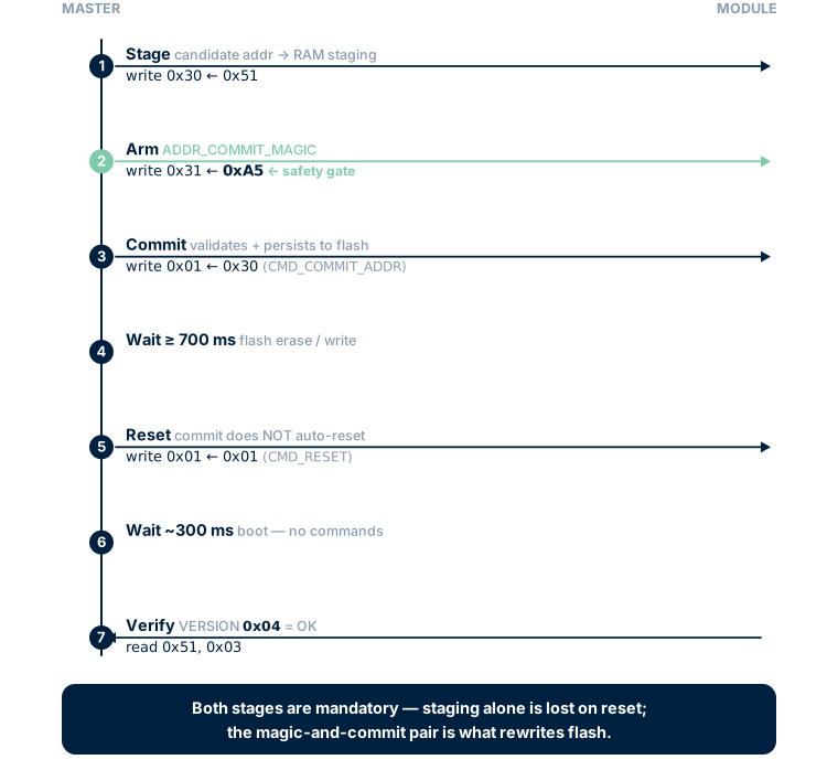
The factory address 0x50 is stored in the user-config block in flash. v1.3 uses a two-phase commit sequence to make accidental address changes hard: a candidate address goes into a RAM staging register first, has to be armed with a magic byte, and only then is committed to flash by an explicit command. A reset re-enumerates the module at the new address.
Registers and commands
| Name | Address / opcode | Type | Purpose |
|---|---|---|---|
REG_I2C_ADDRESS |
0x30 |
u8 RW | Staging for the candidate address (0x08..0x77). Reads back the active address on boot. |
ADDR_COMMIT_MAGIC |
0x31 |
u8 W | Arm the commit with 0xA5. Consumed (cleared) on the commit attempt. |
CMD_COMMIT_ADDR |
opcode 0x30 written to REG_COMMAND (0x01) |
command | Validates the staged address against the magic, persists to flash. |
CMD_RESET |
opcode 0x01 written to REG_COMMAND (0x01) |
command | Soft reset. Module re-enumerates at the new address after ~300 ms. |
Procedure
- Connect only one module (still on
0x50) to the bus. - Stage the new address:
cpp rb_write_u8(0x50, 0x30, 0x51); // candidate address → RAM staging - Arm the commit:
cpp rb_write_u8(0x50, 0x31, 0xA5); // ADDR_COMMIT_MAGIC - Issue
CMD_COMMIT_ADDR(opcode0x30):cpp rb_write_u8(0x50, 0x01, 0x30); - Wait ≥ 700 ms for the flash erase/write:
cpp delay(700); - Issue
CMD_RESET(opcode0x01) —CMD_COMMIT_ADDRdoes not auto-reset:cpp rb_write_u8(0x50, 0x01, 0x01); - Wait ~300 ms for the boot window. Do not issue commands during this window.
- Verify the module ACKs at the new address:
cpp uint8_t ver = rb_read_u8(0x51, 0x03); // VERSION should be 0x04 on v1.3 if (ver == 0x04) Serial.println("Address change OK"); - Mark the PCB with the new address using a wax pencil or label so you can identify the module physically.
Important notes
- Both stages are mandatory. Writing the candidate to
0x30alone does nothing persistent — it only lands in RAM and is lost on the next reset. The magic-and-commit pair is what actually rewrites flash. - The staged address must lie in the range
0x08..0x77(valid 7-bit I²C). Out-of-range writes are rejected withERR_PARAM; the module keeps its current address. - Reserved I²C addresses:
0x00(general-call, see below),0x01..0x07(CBus reserved),0x78..0x7F(10-bit reserved). Do not use these. REG_I2C_ADDRESSreads back the active (running) address, not the staged candidate. To check what is queued for the next reset, you can re-read0x30immediately after staging — it returns the staged value until the next reset.
Full address-change example
#include <Wire.h>
bool change_address(uint8_t old_addr, uint8_t new_addr) {
  if (new_addr < 0x08 || new_addr > 0x77) {
    Serial.println("ERROR: invalid address");
    return false;
  }
  Serial.printf("Changing 0x%02X -> 0x%02X\n", old_addr, new_addr);
  rb_write_u8(old_addr, 0x30, new_addr);   // 1. stage candidate
  rb_write_u8(old_addr, 0x31, 0xA5);       // 2. arm magic
  rb_write_u8(old_addr, 0x01, 0x30);       // 3. CMD_COMMIT_ADDR
  delay(700);                              // 4. flash erase/write
  rb_write_u8(old_addr, 0x01, 0x01);       // 5. CMD_RESET (mandatory)
  delay(300);                              // 6. boot window
  Wire.beginTransmission(new_addr);
  if (Wire.endTransmission() == 0) {
    Serial.printf("OK, module now at 0x%02X\n", new_addr);
    return true;
  }
  Serial.printf("FAIL: module not found at 0x%02X\n", new_addr);
  return false;
}
void setup() {
  Serial.begin(115200);
  Wire.begin();
  delay(300);
  change_address(0x50, 0x51);
}
General Call (broadcast at address 0x00)
The I²C protocol reserves address 0x00 (general call) — frames sent to this address are received by all slaves on the bus simultaneously. rbAmp can latch its per-period snapshot on a general-call frame, but only after the feature has been explicitly enabled on the module.
Opt-in enable (default OFF)
GC latch reception is disabled by default — a fresh module will NACK the general-call frame, which the master detects as a hard error and falls back to per-module sequential latch automatically. To enable GC on a module:
- Set bit 0 of
FLEET_CONFIG:cpp rb_write_u8(0x50, 0x27, 0x01); // bit0 = GC_ENABLE
Note on the value
0x27: this is the register address ofFLEET_CONFIG. The same byte value0x27also happens to be the command opcode forCMD_LATCH_PERIOD(a separate namespace — opcodes go intoREG_COMMANDat0x01). The collision is purely cosmetic; the address and opcode are never confused at the wire level. 2. (Optional) setGROUP_IDfor fleet partitioning —0x00accepts all-call:cpp rb_write_u8(0x50, 0x28, 0x00); // all-call3. Persist:cpp rb_write_u8(0x50, 0x01, 0x32); // CMD_SAVE_USER_CONFIG delay(700);4. Reset and verify the bit landed:cpp rb_write_u8(0x50, 0x01, 0x01); // CMD_RESET delay(300); uint8_t cfg = rb_read_u8(0x50, 0x27); if (cfg & 0x01) Serial.println("GC enabled");
GC frame format
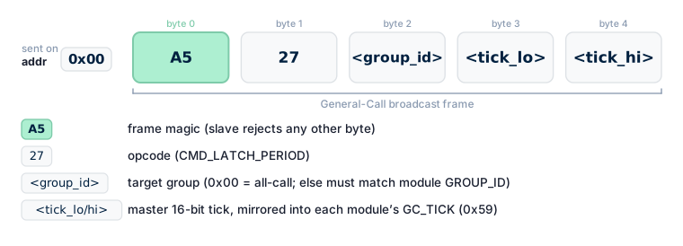
GC latch frames have a fixed magic-and-opcode layout:
addr 0x00 | A5 27 <group_id> <tick_lo> <tick_hi>A5— frame magic (the slave rejects any other byte).27— opcode (CMD_LATCH_PERIOD).<group_id>— target group (0x00= all-call; otherwise must match the module'sGROUP_ID).<tick_lo/hi>— master-side 16-bit tick counter, mirrored into each module'sGC_TICK (0x59)register for missed-frame detection.
By design GC frames carry only latch — destructive opcodes (SAVE_*, COMMIT_ADDR, FACTORY_RESET) are not honoured over general-call.
Broadcast LATCH example (after enable)
// All modules with GC enabled latch their snapshot at once.
Wire.beginTransmission(0x00);
Wire.write(0xA5);                       // frame magic
Wire.write(0x27);                       // CMD_LATCH_PERIOD opcode
Wire.write(0x00);                       // group_id = all-call
Wire.write(tick & 0xFF);                // tick_lo
Wire.write((tick >> 8) & 0xFF);         // tick_hi
uint8_t rc = Wire.endTransmission();
if (rc != 0) {
  // NACK at GC level → no module on the bus has GC enabled.
  // Fall back to per-module sequential LATCH.
}
After the broadcast, each module updates its snapshot independently. The master then reads each module by its individual address. Witness check (recommended): after ~50 ms settle, read V03_PERIOD_VALID (0x07) on each expected module — 1 confirms the latch landed; 0 falls back to per-module latch on that module only.
Application: precise period synchronisation for multi-module energy balancing (e.g. mains_input − solar_output), where the latch instant must be identical across modules.
Recommended multi-module deployment workflow
Step 1: Unbox all modules — every module is on address 0x50.
Step 2: For each module, one at a time:
   a) Connect only this module to the bus.
   b) If the SKU has a plug-in CT: set SENSOR_CLASS (0x25), stage CT_MODEL (0x05),
      issue CMD_SET_CT_MODEL_CHn for each channel, then CMD_SAVE_USER_CONFIG.
   c) Run change_address(0x50, <new_address>).
   d) Verify the module responds at the new address.
   e) Physically mark the module (label with 0x51, 0x52, ...).
   f) Disconnect and move to the next module.
Step 3: After readdressing all modules, connect them in parallel.
        If more than one module is on the bus, cut the built-in pull-up
        jumpers on all but one (see 01_hardware.md → I2C pull-ups).
Step 4: At master boot, run a scan loop and verify every readdressed
        module responds at its expected address.
Module variant auto-detection
⚠ Do not detect the variant by probing for a NACK on register reads. The firmware never NACKs on register reads — unmapped addresses return
0x00(see chapter 11 §5.2). A NACK-based check always reports "channel present".
Use the canonical pair HW_VARIANT (0x55) + CAPABILITY (0x57/0x58):
struct VariantInfo {
  uint8_t hw_variant;     // 1=UI1, 2=UI2, 3=UI3, 4=I1, 5=I2, 6=I3
  uint8_t n_current;      // 1..3
  bool    has_voltage;    // true on UI*, false on I*
};
VariantInfo detect_variant(uint8_t addr) {
  VariantInfo v = {0, 0, false};
  uint8_t product = rb_read_u8(addr, 0x54);             // PRODUCT_ID
  if (product != 0x01) return v;                         // not an rbAmp sensor
  v.hw_variant = rb_read_u8(addr, 0x55);                 // HW_VARIANT
  uint8_t hw = v.hw_variant;
  v.n_current = (hw == 1 || hw == 4) ? 1
              : (hw == 2 || hw == 5) ? 2
              : (hw == 3 || hw == 6) ? 3 : 0;
  uint8_t cap_hi = rb_read_u8(addr, 0x58);               // CAPABILITY high byte
  v.has_voltage = (cap_hi & 0x01) != 0;                  // bit 8 of u16 = voltage-HW
  return v;
}
HW_VARIANT 1..3 are UI-variants (has_voltage == true); 4..6 are I-only variants (has_voltage == false). Mismatch between HW_VARIANT family and CAPABILITY.bit8 indicates a broken / mis-flashed module.
AC_FREQ (0x20) works on all variants — the zero-cross signal comes from a dedicated mains-ZC pin independent of the voltage front-end.
Next
- 03_realtime_polling.md — real-time polling in depth (200 ms window, DRDY)
- 04_period_metering.md — tariff energy accumulation